Monday, April 1, 2013
Fire Stick Schematic Diagram
This article will show you how to build your own version of the Fire-Stick infrared remote control system. The LITEON infrared receiver modules originally designed-in to the Fire-Stick have been discontinued, and forced us to re-design the original circuit boards.
The transmitter schematics.
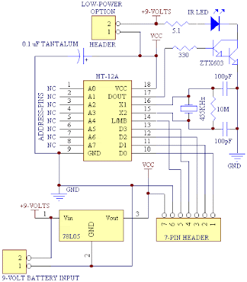

The principle works of the fire stick is the heart of the Fire-Stick is the Holtek HT-12A encoder IC. This handy little encoder was specifically designed for infrared transmission media, and internally generates the 38 KHz carrier frequency for each data transmission.
The data pins of the HT-12A act as both data input pins & transmit enable inputs. Unlike most ordinary encoder ICs with separate transmit enable pins, and data input pins, the HT-12A uses the data input pins to take care of both input functions.
By pulling one of the data pins to ground, the transmission cycle is started. As with most encoders, a pre-determined sequence of events takes place during each separate transmission cycle. The HT-12A however, has a few internal extras that make it pretty flexible. Notice from the flow chart below that the logic state of the L/MB pin is checked prior to finishing the transmission cycle and returning to standby mode.
To L/MB or not to L/MB:
The L/MB pin serves as the Latch/Momentary selection pin, and determines whether the HT-12A will end each transmission cycle by sending the exact logic state present on each data pin, or end the transmission cycle by sending logic "1" 7 times as the data. If L/MB is left floating, (not connected), the transmission will send only the actual logic values present on each of the HT-12A data input pins. This logic value will be latched onto the output pins of the HT-12D decoder IC until you send another transmission with different data.
The HT-12D decoder IC used on the Fire-Stick receiver normally operates in latched mode. Without the added feature of the L/MB function of the HT-12A encoder IC, the receiver would normally operate in latched mode. Operation of the transmitter causes corresponding data pins of the HT-12D decoder IC to latch at logic 0, or logic 1, depending on the actual logic values present on the HT-12A data input pins, and the state of the L/MB pin.
Using the L/MB option of the HT-12A to select momentary operation of the HT-12D will allow the receiver output pins to be momentarily pulsed low, and then return to logic 1 once the transmission ends, and you release the HT-12A data input pin from ground.
The logic state of all address pins on both the encoder & decoder ICs must be 100% identical or no change will be seen on the decoder output pins. The address pins allow for a certain degree of security, and are beneficial if a similar transmitter will be operated within range of your receiver. This simple method also provides an efficient means of controlling multiple receivers in close proximity to one another with a single transmitter.
With different addresses on multiple receivers you need only adjust the address of the transmitter to match that of each receiver to gain control of that receiver. With 8 address pins, A0 - A7, a total of 256 possible address combinations are possible. This means you can control up to 256 separate receivers with a single transmitter, or have up to 256 possible security addresses for a transmitter/receiver combination.
No comments:
Post a Comment
Note: Only a member of this blog may post a comment.