Showing posts with label usb. Show all posts

Wednesday, August 14, 2013

USB Converter


Does this sound familiar: you buy a small piece of equipment, such as a programming & debugging interface for a microcontroller, and you have to use a clunky AC wall adapter to supply it with power? It’s even worse when you’re travelling and there’s no mains socket anywhere in sight. Of course, you can use the USB bus directly as a power source if the supply voltage is 5 V. If you need a higher voltage, you can use the USB converter described here. This small switch-mode step-up converter can generate an output voltage of up to 15 V with a maximum output current of 150 mA.
USB Converter
The LM3578 is a general-purpose switchmode voltage converter. Figure 1 shows its internal block diagram. Here we use it as a step-up converter. The circuit diagram in Figure 2 shows the necessary components. Voltage conversion is achieved by switching on the internal transistor until it is switched off by the comparator or the current-limiting circuit. The collector current flows through coil L1, which stores energy in the form of a magnetic field. When the internal transistor is switched off, the current continues flowing through L1 to the load via diode D1. However, the voltage across the coil reverses when this happens, so it is added to the input voltage. The resulting output voltage thus consists of the sum of the input voltage and the induced voltage across the coil.

USB Converter Circuit
The output voltage depends on the load current and the duty cycle of the internal transistor. Voltage divider R5/R6 feeds back a portion of the output voltage to the comparator in the IC in order to regulate the output voltage. C5 determines the clock frequency, which is approximately 55 kHz. Network R4, C2 and C3 provides loop compensation. The current-sense resistor for the current-limiting circuit is formed by three 1-Ω resistors in parallel (R1, R2 and R3), since SMD resistors with values less than 1 Ω are hard to find. The output voltage ripple is determined by the values and internal resistances of capacitors C11, C8, C7 and C6.
  USB Converter Circuit Diagram

The total effective resistance is reduced by using several capacitors, and this also keeps the construction height of the board low. L2, C1, C9 and C10 act as an input filter. Ensure that the DC resistance of coil L2 is no more than 0.5 Ω. Use a Type B PCB-mount USB connector for connection to the USB bus.  A terminal strip with a pitch of 5.08 mm can be used for the output voltage connector. Of course, you can also solder a cable directly to the board. Two additional holes are provided in the circuit board for this purpose. As we haven’t been able to invent a device that produces more energy than it consumes, you should bear in mind that the input current of the circuit is higher than the output current. As a general rule, you can assume that the input current is equal to the product of the output current and the output voltage divided by the input R5 and R6 for other output voltages:
6V: R5 = 47k, R6 = 9,1k
12V: R5 = 110k, R6 = 10k
15V: R5 = 130k, R6 = 9,1k
voltage and divided again by 0.8. Specifically, with an output current of 100 mA at 9 V, the input current on the USB bus is approximately 225 mA. Finally, Figure 3 shows a small PCB layout for the circuit. All of the components except the connector and the terminal strip are SMDs.
USB Converter pcb
Parts List:
(for UO = 9 V)
Resistors
R1,R2,R3 = 1Ω
R4 = 220kΩ
R5 = 82kΩ
R6 = 10kΩ
Capacitors
(SMD 1206)
C1 = 100nF
C2 = 2nF2
C3 = 22pF
C4 = 100nF
C5 = 1nF5
(tantalum SMD 7343)
C6 = 68μF 20V
C7 = 68μF 20V
C8 = 68μF 20V
C9 = 47μF 16V
C10 = 47μF 16V
C11 = 68μF 20V
Inductors
L1 = 820μH (SMD CD105)
L2 = 47μH (SMD 2220)
Semiconductors
D1 = SK34SMD (Schottky)
IC1 = LM3578AM (SMD SO8)
Miscellaneous
K1 = 2-way PCB terminal block, lead pitch 5mm
(optional)
K2 = USB-B connector

PCB layout, free download from Elektor website, 070119-1.pdf
Author : Jörg Schnyder  copyright : Elektor
[Continue reading]

Sunday, April 7, 2013

Properties and USB Capability
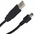

  • Easily connected to the computer because it does not need to open the computer cover. Uniform shape USB connector, there are only two forms of type socket.
  • Hot-plugable - that USB devices can be connected when the computer is on
  • Plug and Play - USB equipment that is easy to use, when connected to a computer, the computer will recognize the pick up program (driver) in accordance with the equipment.
  • Equipment that requires little resources, can take resources from the USB port. Resources off equipment when not in use.
  • High-speed data transfer, can reach 12Mbps.
  • One USB port can be connected with 127 tools.

  • Properties and USB Capability
    USB Cable 

  • Has a fault monitoring and data transmission will be repeated to ensure reliability of data.
  • [Continue reading]

    Sunday, March 31, 2013

    USB Operated Home Appliances Cicuit

    When turning a computer on and off, various peripherals (such as printers, screen, scanner, etc.) often have to be turned on and off as well. By using the 5-V supply voltage from the USB interface on the PC, all these peripherals can easily be switched on and off at the same time as the PC. This principle can also be used with other appliances that have a USB interface (such as modern TVs and radios). This so-called ‘USB-standby-killer’ can be realized with just 5 components. The USB output voltage provides for the activation of the triac opto-driver (MOC3043) which has zero-crossing detection. This, in turn, drives the TRIAC, type BT126.

    Circuit diagram:

    usb-standby-killer-circuit-diagram

    USB Operated Home Appliances Circuit Diagram

    The circuit shown is used by the author for switching loads with a total power of about 150 W and is protected with a 1-A fuse. The circuit can easily handle much larger loads however. In that case and/or when using a very inductive load a so-called snubber network is required across the triac. The value of the fuse will also need to be changed as appropriate. The circuit can easily be built into a mains multi-way powerboard. Make sure you have good isolation between the USB and mains sections.

    Source : www.extremecircuits.net

    [Continue reading]

    Saturday, March 30, 2013

    12 volt DC Power Supply from USB port

    Description :


    Using this circuit we can convert 5V DC from the computer USB port to 12V DC and a circuit like this will find a lot of application in USB powered systems. The heart of this circuit is IC LT1618 which is a constant current, constant voltage boost converter. The IC has a wide input voltage range of 1.8 to 18V DC and output voltage can be up to 35V DC.
    In the circuit resistors R1, R2 sets the output voltage. Pin number 9 is the shutdown pin, less than 0.3V to this pin will shut down the IC. Pin number four is the current sense adjust pin. The current sense voltage can be reduced by applying a DC voltage to this pin. If this adjustment is not needed connect this pin to ground and you can omit components R3, R5 and Q1.
    Circuit diagram of 12 volts dc power supply:
    5volts to 12 volts voltage converter
    Circuit Diagram-12Volts DC power supply from USB port
    Notes :
    • C2 and C3 must be rated at least 15V.
    • Less than 0.3V at the shutdown pin will shutdown the IC.
    • Output voltage is governed by the following equation R1 = R2 (  (Vout /1.263V) -1).

    Other Circuits Related to Power

    [Continue reading]

    Monday, March 25, 2013

    USB Powered Audio Power Amplifier

    This circuit of multimedia speakers for PCs has single-chip-based design, low-voltage power supply, compatibility with USB power, easy heat-sinking, low cost, high flexibility and wide temperature tolerance. At the heart of the circuit is IC TDA2822M. This IC is, in fact, mono-lithic type in 8-lead mini DIP package. It is intended for use as a dual audio power amplifier in battery-powered sound players. Specifications of TDA2822M are low quiescent current, low crossover distortion, supply voltage down to 1.8 volts and minimum output power of around 450 mW/channel with 4-ohm loudspeaker at 5V DC supply input.

    An ideal power amplifier can be simply defined as a circuit that can deliver audio power into external loads without generating significant signal distortion and without consuming excessive quiescent current. This circuit is powered by 5V DC supply available from the USB port of the PC. When power switch S1 is flipped to ‘on’ position, 5V power supply is extended to the circuit and power-indicator red LED1 lights up instantly. Resistor R1 is a current surge limiter and capacitors C1 and C4 act as buffers. Working of the circuit is simple. Audio signals from the PC audio socket/headphone socket are fed to the amplifier circuit through components R2 and C2 (left channel), and R3 and C3 (right channel)

    USB Powered Audio Power Amplifier Circuit diagram:

    USB Powered Audio Power Amplifier Circuit Diagram

    Potmeter VR1 works as the volume controller for left (L) channel and potmeter VR2 works for right (R) channel. Pin 7 of TDA2822M receives the left-channel sound signals and pin 6 receives the right-channel signals through VR1 and VR2, respectively. Ampl i f ied signals for driving the left and right loudspeakers are available at pins 1 and 3 of IC1, respectively. Components R5 and C8, and R6 and C10 form the traditional zobel network. Assemble the circuit on a medium-size, general-purpose PCB and enclose in a suitable cabinet. It is advisable to use a socket for IC TDA2822M. The external connections should be made using suitably screened wires for better result.
    Sucre:  http://www.ecircuitslab.com/2011/06/usb-powered-audio-power-amplifier.html
    [Continue reading]